Karatsuba Multiplier
Problem Statement: Design and simulate a 16-bit Karatsuba Multiplier.
What is Karatsuba Multiplier?
n-digit numbers to three multiplications of n/2-digit numbers.It performs a repeated or recursive reduction to single-digit multiplications.
Lets understand this algorithm before we start designing its datapath.
Let x and y be two n-digit strings in some base B. We can re-write these numbers as follow:
$$x = x_1B^m + x_0,$$ $$y = y_1B^m + y_0,$$
where x0 and y0 are less than Bm. The product is then
$$ \begin{align*} xy &= (x_1B^m + x_0)(y_1B^m + y_0)\newline &= x_1y_1B^{2m} + (x_1y_0 + x_0y_1)B^m + x_0y_0\newline &= t_2B^{2m} + t_1B^m + t_0 \end{align*} $$
where
$$ \begin{align*} t_2 &= x_1y_1\newline t_1 &= x_1y_0 + x_0y_1\newline t_0 &= x_0y_0 \end{align*} $$
Now this formulae requires four multiplications.
As we know multiplier is one of the heavily compute operation in digital logic design. Reducing these operations even by one will improve your circuit's performance and will consume less area.
Karatsuba observed that xy can be computed iBn only three multiplications, at the cost of few extra additions. With t2 and t0 as before and t3 = (x1 + x0) (y1 + y0), one can observe that
$$ \begin{align*} t_1 &= x_1y_0 + x_0y_1\newline &= (x_1 + x_0)(y_1 + y_0) - x_1y_1 - x_0y_0\newline &= t_3 - t_2 - t_0 \end{align*} $$
Thus, only three multiplications are required for computing t2, t1 and t0.
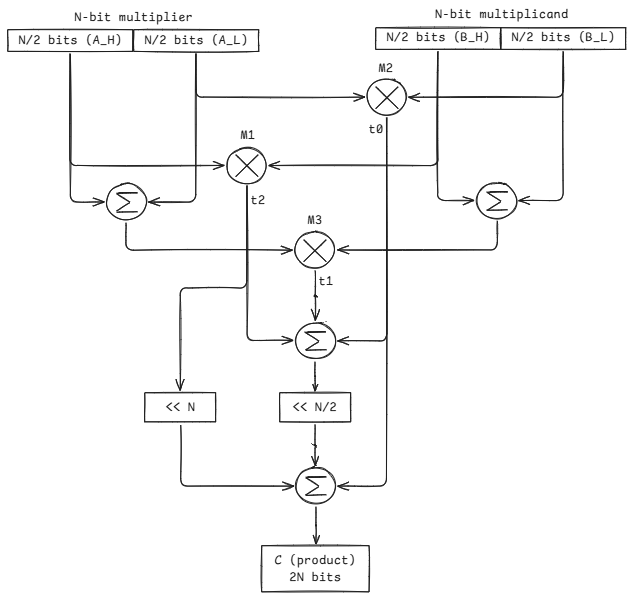
Datapath design of Karatsuba multiplier
-
Now we can draw our datapath based on the above equations. We will require the following components:
- 3 multiplier blocks
- few adders/subtractors
- few logical shift blocks to compute final product
-
The datapath design will look like this.
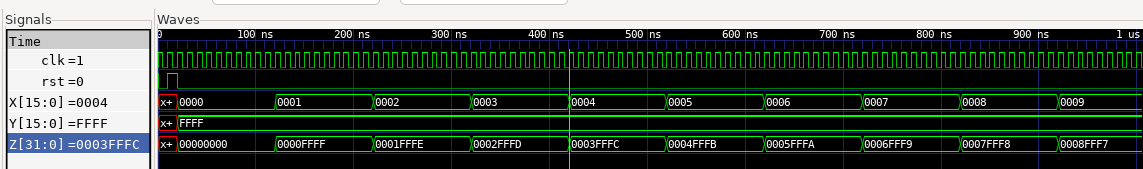
Implementing a 16-bit recursive Karatsuba multiplier
-
Download the Verilog design,
combinational_karatsuba.vfrom here.You will observe that this is a recursive design, meaning the 16-bit multiplier instantiates the 8-bit multiplier, which in turn instantiates a 4-bit multiplier and a 4-bit multiplier instantiates a 2-bit multiplier.
-
Download the testbench design,
tb_combinational_karatsuba.vfrom here. -
Compile the code and check for any syntax errors using the below command.
iverilog combinational_karatsuba.v tb_combinational_karatsuba.v -o combinational_karatsuba -
If there are no errors, use the below command for running the simulation.
vvp combinational_karatsubaYou will see the values of signals being monitored across each clocktick.
-
If all looks well, use the below command for viewing the waveform. Add the signals from
tb_combinational_karatsubadesign to the window to view the simulation output as shown in below image.gtkwave combinational_karatsuba.vcd